 | –≠–ª–µ–∫—Ç—Ä–æ–Ω–Ω—ã–π –∫–æ–º–ø–æ–Ω–µ–Ω—Ç: AD1878 | –°–∫–∞—á–∞—Ç—å:  PDF PDF  ZIP ZIP |
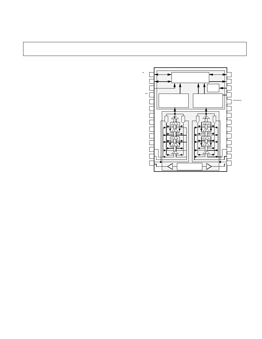
FUNCTIONAL BLOCK DIAGRAM
1
2
3
4
5
6
7
8
9
10
11
12
13
14
28
27
26
25
24
23
22
21
20
19
18
17
16
15
LRCK
BCK
S0
DV
DD
64/32
DGND
NC
AV
SS
1
AV
SS
2
AGND
APD
VINR≠
VINR+
REFR
WCK
DATA
CLOCK
S1
DGND
DV
DD
AV
SS
1
AV
DD
2
AV
DD
1
AGND
VINL≠
VINL+
REFL
VOLTAGE
REFERENCE
SERIAL OUTPUT
INTERFACE
SINGLE-STAGE,
4k-TAP
FIR DECIMATION
FILTER
D
A
C
DIGITAL
CHIP
ANALOG
CHIP
RESET
SINGLE-STAGE,
4k-TAP
FIR DECIMATION
FILTER
D
A
C
D
A
C
D
A
C
REV. 0
Information furnished by Analog Devices is believed to be accurate and
reliable. However, no responsibility is assumed by Analog Devices for its
use, nor for any infringements of patents or other rights of third parties
which may result from its use. No license is granted by implication or
otherwise under any patent or patent rights of Analog Devices.
a
High Performance
16-/18-Bit
Stereo ADCs
AD1878/AD1879*
One Technology Way, P.O. Box 9106, Norwood, MA 02062-9106, U.S.A.
Tel: 617/329-4700
Fax: 617/326-8703
FEATURES
Fully Differential Dual Channel Analog Inputs
103 dB Signal-to-Noise (AD1879 typ)
≠98 dB THD+N (AD1879 typ)
0.001 dB Passband Ripple and 115 dB Stopband
Attenuation
Fifth-Order, 64 Times Oversampling
Modulator
Single Stage, Linear Phase Decimator
256 F
S
Input Clock
APPLICATIONS
Digital Tape Recorders
Professional, DCC, and DAT
A/V Digital Amplifiers
CD-R
Sound Reinforcement
PRODUCT OVERVIEW
The AD1879 is a two-channel, 18-bit oversampling ADC based
on
technology and intended primarily for digital audio appli-
cations. The AD1878 is identical to the 18-bit AD1879 except
that it outputs 16-bit data words. Statements in this data sheet
should be read as applying to both parts unless otherwise noted.
Each input channel of these ADCs is fully differential. Each
data conversion channel consists of a fifth order one-bit noise
shaping modulator and a digital decimation filter. An on-chip
voltage reference provides a voltage source to both channels sta-
ble over temperature and time. Digital output data from both
channels is time-multiplexed to a single, flexible serial interface.
The AD1878/AD1879 accepts a 256
◊
F
S
input master clock.
Input signals are sampled at 64
◊
F
S
on switched-capacitors,
eliminating external sample-and-hold amplifiers and minimizing
the requirements for antialias filtering at the input. With simpli-
fied antialiasing, linear phase can be preserved across the passband.
The AD1878/AD1879's proprietary fifth-order differential
switched-capacitor modulator architecture shapes the one-bit
comparator's quantization noise out of the audio passband. The
high order of the modulator randomizes the modulator output,
reducing idle tones in the AD1878/AD1879 to very low levels.
The AD1878/AD1879's differential architecture provides in-
creased dynamic range and excellent common-mode rejection
characteristics. Because its modulator is single-bit, AD1878/
AD1879 is inherently monotonic and has no mechanism for
producing differential linearity errors.
The digital decimation filters are single-stage, 4095-tap finite
impulse response filters for filtering the modulator's high fre-
quency quantization noise and reducing the 64
◊
F
S
single-bit
output data rate to a F
S
word rate. They provide linear
*
Protected by U.S. Patent Numbers 5055843, 5126653, and others pending.
phase and a narrow transition band that permits the digitization
of 20 kHz signals while preventing aliasing into the passband
even when using a 44.1 kHz sampling frequency. Passband
ripple is less the 0.001 dB, and stopband attenuation exceeds
115 dB.
The flexible serial output port produces data in twos-complement,
MSB-first format. Input and output signals are to TTL and
CMOS-compatible logic levels. The port is configured by pin
selections. The AD1878/AD1879 can operate in either master
or slave mode. Each 16-/18-bit output word of a stereo pair can
be formatted within a 32-bit field as either right-justified, I
2
S-
compatible, or at user-selected positions. The output can also be
truncated to 16-bits by formatting into a 16-bit field.
The AD1878/AD1879 consists of two integrated circuits in a
single ceramic 28-pin DIP package. The modulators and refer-
ence are fabricated in a BiCMOS process; the decimator and
output port, in a 1.0
µ
m CMOS process. Separating these func-
tions reduces digital crosstalk to the analog circuitry. Analog and
digital supply connections are separated to further isolate the
analog circuitry from the digital supplies.
The AD1878/AD1879 operates from
±
5 V power supplies over
the temperature range of ≠25
∞
C to +70
∞
C.

REV. 0
AD1878/AD1879≠SPECIFICATIONS
≠2≠
TEST CONDITIONS UNLESS OTHERWISE NOTED
Supply Voltages
±
5
V
Ambient Temperature
25
∞
C
Input Clock (F
CLOCK
)
12.288
MHz
Input Signal
974
Hz
≠0.5
dB Full Scale
All minimums and maximums tested except as noted.
ANALOG PERFORMANCE
Min
Typ
Max
Units
AD1879 Resolution
18
Bits
AD1878 Resolution
16
Bits
Clock Input Frequency Range
CLOCK Input (F
CLOCK
)
0.01
12.288
14.286
MHz
Modulator Sample Rate (F
CLOCK
/4)
0.0025
3.072
3.5715
MHz
Output Word Rate (F
S
= F
CLOCK
/256)
0.039
48
55.8
kHz
AD1879 Dynamic Range (0 kHz to 20 kHz, ≠60 dB input)
Stereo Mode (No A-Weight Filter)
100
103
dB
Mono Mode
1
(No A-Weight Filter)
106
dB
Stereo Mode (with A-Weight Filter)
105
dB
AD1879 Trimmed
2
Signal to (Noise + Distortion)
Full Scale
93
98
dB
≠20 dB
83
dB
AD1879 Untrimmed
3
Signal to (Noise + Distortion)
Full Scale
91
96
dB
≠20 dB
83
dB
AD1879 Trimmed
2
Signal to Total Harmonic Distortion
Full Scale
98
dB
≠20 dB
100
dB
AD1878 Dynamic Range (0 kHz to 20 kHz, ≠60 dB 1.0936 kHz
Input Dithered with a ≠10 dB 21.873 kHz Sine Wave)
Stereo Mode (No A-Weight Filter)
95
97
dB
AD1878 Trimmed
2
Signal to (Noise + Distortion)
Full Scale
93
95
dB
≠20 dB
77
dB
AD1878 Untrimmed
3
Signal to (Noise + Distortion)
Full Scale
91
94
dB
≠20 dB
77
dB
AD1878 Trimmed
2
Signal to Total Harmonic Distortion
Full Scale
98
dB
≠20 dB
100
dB
Analog Inputs
Differential Input Range
4
±
5.985
±
6.3
±
6.615
V
Input Impedance at Each Input Pin
7.0
k
DC Accuracy
Gain Error
±
1
±
5
%
Interchannel Gain Mismatch
0.05
0.15
dB
Gain Drift
150
ppm/
∞
C
AD1879 Midscale Offset Error
±
200
±
750
18-Bit LSBs
AD1878 Midscale Offset Error
±
50
±
200
16-Bit LSBs
Midscale Drift
13
ppm/
∞
C
Voltage Reference
2.4
2.86
3.2
V
Crosstalk (EIAJ Method)
100
105
dB
Interchannel Phase Deviation
±
0.001
Degrees
NOTES
1
Both channels connected together for mono operations as described below in "How to Extend SNR."
2
Differential gain imbalance manually trimmed to eliminate second harmonic. See "Applications Issues" below.
3
Test performed without part-to-part trimming.
4
The differential input range is twice the range seen at each input pin. The input range corresponds to the full-scale digital output range.
Specifications subject to change without notice.
AD1878/AD1879
DIGITAL INPUTS
Min
Max
Units
V
IH
V
V
IL
0.8
V
I
IH
@ V
IH
= 5 V
10
µ
A
I
IL
@ V
IL
= 0 V
10
µ
A
V
OH
@ I
OH
= 360
µ
A
4.0
V
V
OL
@ I
OL
= 1.6 mA
0.5
V
DIGITAL TIMING
Min
Typ
Max
Units
CLOCK
Period (T
CLOCK
= 1/F
CLOCK
)
0.07
100
µ
s
LO Pulse Width
35
ns
HI Pulse Width
35
ns
BCK Pulse Width
2
CLOCK Periods
64-Bit Frame LRCK Pulse Width
32
BCK Periods
32-Bit Frame LRCK Pulse Width
16
BCK Periods
WCK Pulse Width
1
BCK Periods
t
RSET
RESET
Setup to CLOCK Rising
5
ns
t
RHLD
RESET
Hold from CLOCK Rising
20
ns
t
RSLS
RESET
Pulse Width
4
10
µ
s
CLOCK Periods
t
WSET
WCK to CLOCK Rising
5
ns
t
WHLD
WCK Hold from CLOCK Rising
20
ns
t
DLYCK
CLOCK to BCK/WCK/LRCK Delay
65
ns
(Master Mode)
t
SET
BCK/LRCK to CLOCK Falling
5
ns
(Slave Mode)
t
HLD
BCK/LRCK Hold from CLOCK Falling
20
ns
(Slave Mode)
t
DLYD,
MSB
CLOCK Falling to MSB DATA Delay
65
ns
t
DLYD
CLOCK Rising to DATA Delay, Except MSB
70
ns
POWER
Min
Typ
Max
Units
Supplies
Voltage, DV
DD
/AV
DD
1/AV
DD
2
4.75
5
5.25
V
Voltage, AV
SS
1/AV
SS
2
≠5.25
≠5
≠4.75
V
Current, AV
DD
1/AV
SS
1
73
92
mA
Current, AV
DD
1/AV
SS
1--Power Down
13
23
mA
Current, AV
DD
2/AV
SS
2
8
10
mA
Current, DV
DD
64
70
mA
Dissipation
Operation
1,130
1,370
mW
Operation--Analog Supplies
810
1,020
mW
Operation--Digital Supplies
320
350
mW
Power Down (All Supplies)
530
680
mW
Power Supply Rejection
1 kHz 300 mV p-p Signal at Analog Supply Pins
102
dBFS
Passband--Any 300 mV p-p Signal
92
dBFS
Stopband--Any 300 mV p-p Signal
105
dBFS
TEMPERATURE RANGE
Min
Typ
Max
Units
Specifications Guaranteed
+25
∞
C
Functionality Guaranteed
≠25
+70
∞
C
Storage
≠60
+100
∞
C
REV. 0
≠3≠
AD1878/AD1879
REV. 0
≠4≠
ABSOLUTE MAXIMUM RATINGS
Min
Typ
Max
Units
DV
DD
to DGND and AV
DD
1/AV
DD
2 to AGND
0
6
V
AV
SS
1/AV
SS
2 to AGND
≠6
0
V
AV
SS
2 to AV
SS
1
≠0.3
V
Digital Inputs to DGND
≠0.3
DV
DD
+ 0.3
V
Analog Inputs
AV
SS
1 ≠ 0.3
AV
DD
1 + 0.3
V
AGND to DGND
≠0.3
0.3
V
Reference Voltage
Indefinite Short Circuit to Ground
Soldering
+300
∞
C
10
sec
DIGITAL FILTER CHARACTERISTICS
Min
Typ
Max
Units
Decimation Factor
64
Passband Ripple
0.001
dB
Stopband
1
Attenuation
115
dB
48 kHz F
S
(12.288 MHz CLOCK)
Passband
0
21.7
kHz
Stopband
26.2
3,045
kHz
44.1 kHz F
S
(11.2896 MHz CLOCK)
Passband
0
20.0
kHz
Stopband
24.1
2,798
kHz
32 kHz F
S
(8.192 MHz CLOCK)
Passband
0
14.5
kHz
Stopband
17.5
2,030
kHz
Other F
S
Passband
0
0.4535
F
S
Stopband
0.5458
63.4542
F
S
Group Delay ([4096/2]/[64
◊
F
S
])
32/F
S
Group Delay Variation
0
µ
s
NOTE
1
Stopband repeats itself at multiples of 64
◊
F
S,
where F
S
is the output word rate. Thus the digital filter will attenuate to 115 dB across the frequency spectrum
except for a range
±
0.5458
◊
F
S
wide at multiples of 64
◊
F
S
.
Specifications subject to change without notice.
ORDERING GUIDE
Package
Package
Model
Temperature
Description
Option
AD1878JD
≠25
∞
C to +70
∞
C
Ceramic DIP
D-28
AD1879JD
≠25
∞
C to +70
∞
C
Ceramic DIP
D-28
WARNING!
ESD SENSITIVE DEVICE
CAUTION
ESD (electrostatic discharge) sensitive device. Electrostatic charges as high as 4000 V readily
accumulate on the human body and test equipment and can discharge without detection.
Although the AD1878/AD1879 features proprietary ESD protection circuitry, permanent dam-
age may occur on devices subjected to high energy electrostatic discharges. Therefore, proper
ESD precautions are recommended to avoid performance degradation or loss of functionality.
AD1878/AD1879
REV. 0
≠5≠
DEFINITIONS
Dynamic Range
The ratio of a full-scale output signal to the integrated output
noise in the passband (0 kHz to 20 kHz), expressed in decibels
(dB). Dynamic range is measured with a ≠60 dB input signal
and is equal to (S/[THD+N]) + 60 dB.
Signal to (Noise + Distortion)
The ratio of the root-mean-square (rms) value of the fundamen-
tal input signal to the rms sum of all spectral components in the
passband, expressed in decibels (dB).
Signal to Total Harmonic Distortion (THD)
The ratio of the rms sum of all harmonically related spectral
components in the passband to the fundamental input signal,
expressed either as a percentage (%) or in decibels (dB).
Passband
The region of the frequency spectrum unaffected by the attenu-
ation of the digital decimator's filter.
Passband Ripple
The peak-to-peak variation in amplitude response from equal
amplitude input signal frequencies within the passband, ex-
pressed in decibels.
Stopband
The region of the frequency spectrum attenuated by the digi-
tal decimator's filter to the degree specified by "stopband
attenuation."
Gain Error
With a near full-scale input, the ratio of actual output to ex-
pected output, expressed as a percentage.
Interchannel Gain Mismatch
With near full-scale inputs, the ratio of outputs of the two stereo
channels, expressed in decibels.
Gain Drift
Change in response to a near full-scale input with a change in
temperature, expressed as parts-per-million (ppm) per
∞
C.
Midscale Offset Error
Output response to a midscale input (i.e., zero volts dc), ex-
pressed in least-significant bits (LSBs).
Midscale Drift
Change in midscale offset error with a change in temperature,
expressed as parts-per-million (ppm) of full scale per
∞
C.
Crosstalk
Ratio of response on one channel with a grounded input to a
full-scale 1 kHz sine-wave input on the other channel, expressed
in decibels.
Interchannel Phase Deviation
Difference in input sampling times between stereo channels, ex-
pressed as a phase difference in degrees between 1 kHz inputs.
Power Supply Rejection
With analog inputs grounded, energy at the output when a
300 mV p-p signal is applied to power supply pins, expressed in
decibels of full scale.
Group Delay
Intuitively, the time interval required for an input pulse to ap-
pear at the converter's output, expressed in milliseconds (ms).
More precisely, the derivative of radian phase with respect to
radian frequency at a given frequency.
Group Delay Variation
The difference in group delays at different input frequencies.
Specified as the difference between largest and the smallest
group delays in the passband, expressed in microseconds (
µ
s).
AD1878/AD1879 PIN LIST
Pin Input/Output Pin Name Description
1
1
I/O
LRCK
Left/Right Clock
1
2
I/O
BCK
Bit Clock
1
3
I
S0
Mode Select 0
1
4
I
64/32
Bit Rate Select
1
5
I
DV
DD
+5 V Digital Supply
1
6
I
DGND
Digital Ground
1
7
N/C
No Connection; Do Not Connect
1
8
I
AV
SS
1
≠5 V Analog Supply
1
9
I
AV
SS
2
≠5 V Analog Logic Supply
10
I
AGND
Analog Ground
11
I
APD
Analog Power Down
12
I
VINR≠
Right Inverting Input
13
I
VINR+
Right Noninverting Input
14
I/O
REFR
Right Reference Capacitor
15
I/O
REFL
Left Reference Capacitor
16
I
VINL+
Left Noninverting Input
17
I
VINL≠
Left Inverting Input
18
I
AGND
Analog Ground
19
I
AV
DD
1
+5 V Analog Supply
20
I
AV
DD
2
+5 V Analog Logic Supply
21
I
AV
SS
1
≠5 V Analog Supply
22
I
DV
DD
+5 V Digital Supply
23
I
DGND
Digital Ground
24
I
RESET
Reset
25
I
S1
Mode Select 1
26
I
CLOCK
Master Clock Input
27
O
DATA
Serial Data Output
28
I/O
WCK
Word Clock
THEORY OF OPERATION
Modulator Noise-Shaping
The stereo, differential analog modulators of the AD1878/
AD1879 employ a proprietary feedforward and feedback archi-
tecture that passes input signals in the audio band with a unity
transfer function yet simultaneously shape the quantization
noise generated by the one-bit comparator out of the audio
band. See Figure 1. Without the
architecture, this quantiza-
tion noise would be spread uniformly from dc to one-half the
oversampling frequency, 64
◊
F
S
. (Regardless of architecture,
64 times oversampling by itself significantly reduces the quanti-
zation noise in the audio band if the input is properly dithered.
However, the noise reduction is only [log
2
64]
◊
3 dB = 18 dB.)
PIN 1
0.580 (14.73)
0.485 (12.32)
1
14
15
2
8
0.625 (15.87)
0.600 (15.24)
0.015 (0.381)
0.008 (0.204)
0.195 (4.95)
0.125 (3.18)
0.250
(6.35)
MAX
0.022 (0.558)
0.014 (0.356)
0.100
(2.54)
BSC
0.200 (5.05)
0.125 (3.18)
0.070 (1.77)
MAX
0.060 (1.52)
0.015 (0.38)
0.150
(3.81)
MIN
SEATING
PLANE
1.565 (39.70)
1.380 (35.10)
Figure 1. AD1878/AD1879 Modulator Noise-Shaper (One
Channel)

AD1878/AD1879
REV. 0
≠6≠
The AD1878/AD1879's patented
architectures "shape" the
quantization noise-transfer function in a nonuniform manner.
Through careful design, this transfer function can be specified to
high-pass filter the quantization noise out of the audio band into
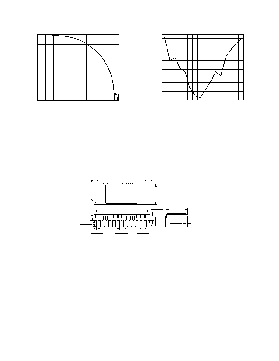
higher frequency regions. See Figure 27. The Analog Devices'
AD1878/AD1879 also incorporates feedback resonators from
the third integrator's output to the second integrator's input and
from the fifth integrator's output to the fourth integrators' input.
These resonators do not affect the signal transfer function but
allow flexible placement of zeros in the noise transfer function.
For the AD1878/AD1879, these zeros were placed near the high
frequency end of the audio passband, reducing the quantization
noise in a region where it otherwise would have been increasing.
Oversampling by 64 simplifies the implementation of a high per-
formance audio analog-to-digital conversion system. Antialias
requirements are minimal; a single pole of filtering will usually
suffice to eliminate inputs near F
S
and its higher multiples.
A fifth-order architecture was chosen both to strongly shape the
noise out of the audio band and to help break up the idle tones
produced in all
architectures. These architectures have a ten-
dency to generate periodic patterns with a constant dc input, a
response that looks like a tone in the frequency domain. These
idle tones have a direct frequency dependence on the input dc
offset and indirect dependence on temperature and time as it
affects dc offset. The human ear operates effectively like a spec-
trum analyzer and can be sensitive to tones below the integrated
noise floor, depending on frequency and level. The AD1878/
AD1879 suppresses idle tones typically 110 dB or better below
full-scale input levels.
Previously it was thought that higher-order modulators could
not be designed to be globally stable. However, the AD1878/
AD1879's modulator was designed, simulated, and exhaustively
tested to remain stable for any input within a wide tolerance of
its rated input range. The AD1878/AD1879 was designed to
reset itself should it ever be overdriven and go unstable. It will
reset itself within 5
µ
s at a 48 kHz sampling frequency. Any such
reset events will be invisible to the user since overdriving the in-
puts will produce a "clipped" waveform at the output.
The AD1878/AD1879 modulator architecture has been imple-
mented using switched-capacitors. A systems benefit is that ex-
ternal sample-and-hold amplifiers are unnecessary since the
capacitors perform the sample-and-hold function Coefficient
weights are created out of varying capacitor sizes. The dominant
noise source in this design is kT/C noise, and the input capaci-
tors are accordingly very large to achieve the AD1878/AD1879's
performance levels. (Each 6 dB improvement in dynamic range
requires a quadrupling of input capacitor size, as well as an
increase in size of the op amps to drive them.) This AD1878/
AD1879 thermal noise has been controlled to properly dither the
input to an 18-bit level. (Note that 16-bit results from either the
AD1878 or AD1879 will be underdithered.)
With capacitors of adequate size and op amps of adequate drive,
a well-designed switched-capacitor modulator will be relatively
insensitive to jitter on the sampling clock. The key issue is
whether the capacitors have had sufficient time to charge or
discharge during the clock period. A properly designed switched
capacitor modulator should be no more sensitive to clock jitter
than are traditional nonoversampled ADCs. This contrasts with
continuous-time modulators, which are very sensitive to the
exact location of sampling clock edges.
See Figures 20≠23 for illustrations of the AD1878/AD1879's
typical analog performance resulting from this design. Signal-
to-noise+distortion is shown under a range of conditions. Note
the very good linearity performance of the AD1878/AD1879 as
a consequence of its single-bit
architecture in Figure 24.
The common-mode rejection (Figure 25) graph illustrates the
benefits of the AD1878/AD1879's differential architecture. The
excellent channel separation shown in Figure 26 is the result of
careful chip design and layout. The relatively small change in
gain over temperature (Figure 31) results from a robust refer-
ence design.
The output of the AD1878/AD1879 modulators is a stereo
bitstream at 64
◊
F
S
(3.072 MHz for F
S
= 48 kHz). Spectral
analysis of these bits would show that they contain a high qual-
ity replica of the input in the audio band and an enormous
amount of quantization noise at higher frequencies. The input
signal can be recreated directly if these bits are fed into a prop-
erly designed analog low-pass filter.
Digital Filter Characteristics
The digital decimator accepts the modulators' stereo bitstream
and simultaneously performs two operations on it. First, the
decimator low-pass filters the quantization noise that the modu-
lator shaped to high frequencies and filters any other out-of-
audio-band input signals. Second, it reduces the data rate to an
output word rate equal to F
S
. The high frequency bitstream is
reduced to stereo 16-/18-bit words at 48 kHz (or other desired
F
S
). The one-bit quantization noise, other high-frequency com-
ponents of the bitstream, and analog signals in the stopband are
attenuated by at least 115 dB.
The AD1878/AD1879 decimator implements a symmetric Finite
Impulse Response (FIR) filter, resulting in its linear phase re-
sponse. This filter achieves a narrow transition band (0.0923
◊
F
S
), high stopband attenuation (> 115 dB), and low passband
ripple (< 0.001 dB). The narrow transition band allows the
unattenuated digitization of 20 kHz input signals with F
S
as low
as 44.1 kHz. The stopband attenuation is sufficient to eliminate
modulator quantization noise from affecting the output. Low
passband ripple prevents the digital filter from coloring the
audio signal. For this level of performance, 4095 22-bit coeffic-
ients (taps) were required in each channel of this filter. The
AD1878/AD1879's decimator employs a proprietary single-
stage, multiplier-free structure developed in conjunction with
Ensoniq Corporation. See Figures 28 and 29 for the digital
filter's characteristics.
The output from the decimator is available as a single serial
output, multiplexed between left and right channels.
Note that the digital filter itself is operating at 64
◊
F
S
. As a
consequence, Nyquist images of the passband, transition band,
and stopband will be repeated in the frequency spectrum at
multiples of 64
◊
F
S
. Thus the digital filter will attenuate to
115 dB across the frequency spectrum except for a window
±
0.5458
◊
F
S
wide centered at multiples of 64
◊
F
S
. Any input
signals, clock noise, or digital noise in these frequency windows
will not be attenuated to the full 115 dB. If the high frequency
signals or noise appear within the passband images within these
windows, they will not be digitally attenuated at all.
AD1878/AD1879
REV. 0
≠7≠
Sample Delay
The sample delay or "group delay" of the AD1878/AD1879 is
dominated by the processing time of the digital decimation fil-
ter. FIR filters convolve a vector representing time samples of
the input with an equal-sized vector of coefficients. After each
convolution, the input vector is updated by adding a new
sample at one end of the "pipeline" and eliminating the oldest
input sample at the other. For an FIR filter, the time at which a
step input appears at the output will be approximately when that
step input is halfway through the input sample vector pipeline.
The input sample vector is updated every 64
◊
F
S
. Thus, the
sample delay will be given by the equation,
Group Delay = (4096 2) /(64
◊
F
S
) = 32 / F
S
For the most common sample rates this can be summarized as:
F
S
Group Delay
48 kHz
667
µ
s
44.1 kHz
725
µ
s
32 kHz
1000
µ
s
Due to the linear phase properties of FIR filters, the group delay
variation, or differences in group delay at different frequencies is
zero.
OPERATING FEATURES
Voltage Reference
The AD1878/AD1879 includes a +3 V on-board reference
which determines the AD1878/AD1879's input range. This ref-
erence is buffered to both channels of the AD1878/AD1879's
modulator, providing a well-matched reference to minimize
interchannel gain mismatch. The reference should be bypassed
with 10
µ
F tantalum capacitors as shown in Figure 2. The inter-
nal reference can be overpowered by applying an external refer-
ence at the REFR (Pin 14) and REFL (Pin 15) pins, allowing
multiple AD1878/AD1879s to be calibrated to the same gain.
Note that the reference pins still must be bypassed as shown.
Sample Clock
An external master clock supplied to CLOCK (Pin 26) drives
the AD1878/AD1879 modulator, decimator, and digital inter-
face. As with any analog-to-digital conversion system, the sam-
pling clock must be low jitter to prevent conversion errors.
The input clock operates at 256
◊
F
S
. The clock is divided down
to obtain the 64
◊
F
S
clock required for the modulator. The out-
put word rate will be at F
S
itself. This relationship is illustrated
for popular sample rates below:
AD1879
Modulator
Output Word
CLOCK Input
Sample Rate
Rate
12.288 MHz
3.072 MHz
48 kHz
11.2896 MHz
2.822 MHz
44.1 kHz
8.192 MHz
2.048 MHz
32 kHz
The AD1878/AD1879 serial interface supports both "master"
and "slave" modes. Note that even in slave mode it is presumed
that the serial interface clocks are derived from the master clock
input, CLOCK. Slave mode does not support asynchronous
data transfers, since asynchronous data transfers would compro-
mise the performance of any high performance converter.
The AD1878/AD1879 decimator makes use of dynamic logic to
minimize die area. There is, therefore, a minimum clock fre-
quency that the AD1878/AD1879 will support specified in
"Specifications" above. Operation of the AD1878/AD1879 at
lower frequencies will cause the device to consume excessive
power and may damage the converter.
Reset
The active LO RESET pin (Pin 24) allows initializing the
AD1879. This is of value only for synchronizing multiple
AD1878/AD1879s in Master Mode--WCK Output. Unless you
are interested in synchronizing multiple AD1878/AD1879s, we
recommend tying RESET HI. The reset function is useful for
nothing else. In fact, there is a maximum specification on
RESET
LO; excessive power consumption may occur with loss
of reliability if left LO too long due to the dynamic logic on the
chip.
Figure 14 illustrates the timing parameters for RESET to
accomplish synchronization of multiple Master Mode--Word
Clock Output ADCs. (This sequence is not necessary for syn-
chronizing multiple AD1878/AD1879s in other modes. See
"Synchronizing Multiple AD1878/AD1879s" below.) Note that
RESET
first has to be LO for at least four CLOCK periods
(three CLOCKs plus t
RSET
plus t
RHLD
, to be more precise).
Then RESET must be HI for a minimum of one CLOCK and a
maximum of two CLOCKs. Then RESET must he LO for at
least another four CLOCKs. From the time when RESET goes
HI again, exactly 127 CLOCKs will occur before LRCK goes
LO.
Analog Power Down
The AD1878/AD1879 features a power-down mode that
reduces current to the analog modulator. It is controlled by
the active HI APD (Pin 11). The power savings are specified in
"Specifications." The converter is still "alive" in the power-
down state but will not produce valid results for all audio-band
inputs.
Power consumption can be further reduced by slowing down
the master clock input to the minimum clock frequency,
F
CLOCK
, specified for the AD1878/AD1879.
APPLICATIONS ISSUES
Recommended Input Structure
The AD1878/AD1879 input structure is fully differential for
improved common-mode rejection properties and increased
dynamic range. Since each input pin sees
±
3 V swings, each
channel's input signal effectively swings
±
6 V, i.e., across a
12 V range.
In most cases, a single-ended-to-differential input circuit is
required. Shown in Figure 2 is our recommended circuit, based
on extensive experimentation. Note that to maximize signal
swing, the op amps in this circuit are powered by
±
12 V or
greater supplies. The AD1878/AD1879 itself requires
±
5 V
supplies. If
±
5 V supplies are not already available in your sys-
tem, Figure 3 illustrates our recommended circuit for generat-
ing these supplies.
AD1878/AD1879
REV. 0
≠8≠
RIGHT INPUT
NE5532 OR OP-275
100pF
.1µF
5.76k
100pF
V
CC
V
SS
249k
100k
249k
V
SS
.1µF
.0047 µF
NPO
.01µF
NPO
.01µF
NPO
NE5532 OR
OP-275
VINR≠
VINR+
VINL+
VINL≠
12
13
16
17
REFR
REFL
10µF
14
.1µF
AD1878/79
LEFT
INPUT
100pF
100pF
V
CC
.1µF
.0047 µF
NPO
.01µF
NPO
NE5532 OR
OP-275
.1µF
V
CC
V
SS
.1µF
.01µF
NPO
10µF
15
5.62k
5.62k
5.62k
5.62k
5.49k
51
51
200
249k
5.62k
100k
5.36k
200
51
51
5.62k
5.62k
5.62k
249k
5.90k
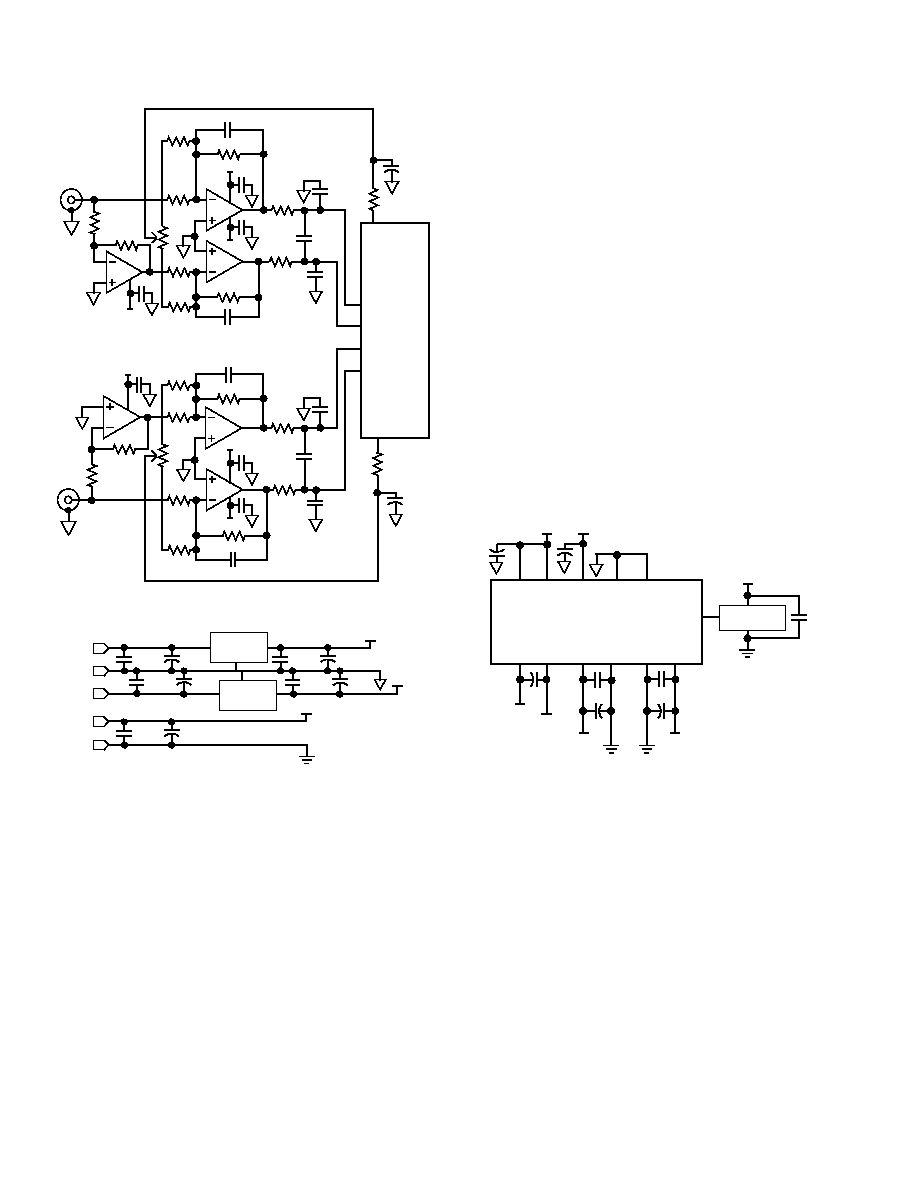
Figure 2. AD1878/AD1879 Recommended Input Structure
V
CC
AGND
V
SS
V
DD
DGND
0.1µF
22µF
7805
IN
OUT
GND
+5V ANALOG
≠5V
ANALOG
+5V DIGITAL
+12V < V
CC
< +18V
≠12V > V
SS
> ≠ 18V
0.1µF
22µF
0.1µF
22µF
7905
IN
OUT
GND
0.1µF
10µF
0.1µF
10µF
Figure 3. AD1878/AD1879 Recommended Power Condi-
tioning Circuit (If
±
5 V Supplies Are Not Already Available)
The trim potentiometers shown in Figure 2 connecting the
minus (≠) inputs of the driving op amps permit trimming out dc
offset, if desired.
Note that the driving op amp feedback resistors are all slightly
different values. These values produce a slight differential gain
imbalance and were derived empirically to minimize second
harmonic distortion on average and produce the best overall
THD without part-by-part trimming. Replacing one of these
feedback resistors in each channel with a trim potentiometer
allows trimming the differential gain imbalance for part-by-part
optimal performance. We have done this in the lab by parallel-
ing 100 k
trim potentiometers around the 5.49 k
and
5.36 k
input feedback resistors for the V
IN
plus (+) signals
that can be found in Figure 2. By trimming gain imbalance, sec-
ond harmonic distortion can always be eliminated. In "Specifi-
cations," a distinction is drawn between trimmed and untrimmed
signal-to (noise + distortion) and trimmed and untrimmed total
harmonic distortion. The untrimmed specifications are tested to
the input structure shown in Figure 2. The trimmed specifica-
tions are based on a part-by-part trim of this differential gain to
eliminate the second harmonic.
The input circuit of Figure 2 could be implemented with a
single pair of operational amplifiers per channel, one inverting
and one noninverting. The recommended architecture shown in
Figure 2 using three inverting op amps per channel provides iso-
lation of the op amp inputs from charge dumped back from the
AD1878/AD1879's input capacitors when these large capacitors
switch. The performance from a two op amp per channel input
structure is not quite as good as the structure recommended,
but it is close and may be adequate in many applications.
Layout and Decoupling Considerations
Obtaining the best possible performance from a state-of-the-art
data converter like the AD1878/AD1879 requires close atten-
tion to board layout. From extensive experimentation, we have
discovered principles that produce typical values of 103 dB dy-
namic range and 98 dB S/(THD+N) in your system. Schematics
of our AD1878/AD1879 Evaluation Board, which implements
these recommendations, are available from Analog Devices.
The principles and their rationales are listed below in descend-
ing order of importance. The first two pertain to bypassing and
are illustrated in Figure 4.
AD1878/ 79
AV
SS
1 AV
SS
1 AV
DD
1 AGND AGND
10µF
≠5V
ANALOG
+5V
ANALOG
10µF
0.1µF
+5V
DIGITAL
10µF
0.1µF
+5V
DIGITAL
AV
SS
2 AV
DD
2 DV
DD
DGND DGND DV
DD
≠5V
ANALOG
+5V
ANALOG
+5V DIGITAL
OSCILLATOR
0.1µF
26
CLKIN
10µF
10µF
8
21
19
10
18
9
20
5
6
23
22
Figure 4. AD1878/AD1879 Recommended Bypassing and
Oscillator Circuits
∑
The digital bypassing of the AD1878/AD1879 is the most
critical item on the board layout. There are two pairs of digi-
tal supply pins of the part, each pair on opposite sides (Pins 5
and 6 and Pins 22 and 23). The user should tie a bypass ca-
pacitor set (0.1
µ
F ceramic and 10
µ
F tantalum) on EACH
pair of supply pins as close to the pins as possible. The traces
between these package pins and the capacitors should be as
short and as wide as possible. This will prevent digital supply
current transients from being inductively transmitted to the
inputs of the part.
∑
The analog input bypassing is the second most critical item.
Use 0.01
µ
F NPO ceramic capacitors from each input pin to
the analog ground plane, with a clear ground path from the
bypass capacitor to the AGND pin on the same side of the
package (Pins 10 and 18). The trace between this package
pin and the capacitor should be as short and as wide as pos-
sible. A 0.0047
µ
F NPO ceramic capacitor should be placed
AD1878/AD1879
REV. 0
≠9≠
between each set of input pins (12 to 13, and 17 to 16) to
complete the input bypassing. This input bypassing mini-
mizes the RF transmission and reception capability of the
AD1878/AD1879 inputs.
∑
For best performance, do not use a socket with the AD1878/
AD1879. If you must socket the part, use pin clips to keep
the part flush with the board, thus keeping bypassing as
close to the chip as possible.
∑
The AD1878/AD1879 should be placed on a split ground
plane as illustrated in Figure 5. The digital ground plane
should be placed under the top end of the package and the
analog ground plane should be placed under the bottom end
of the package as shown in Figure 5. The split should be be-
tween Pins 7 and 8 and between Pins 21 and 22. The
ground planes should be tied together at one spot under-
neath the center of the package. This ground plane tech-
nique also minimizes RF transmission and reception.
1
2
3
4
5
6
7
8
9
10
11
12
13
14
28
27
26
25
24
23
22
21
20
19
18
17
16
15
LRCK
BCK
S0
DV
DD
64/32
DGND
NC
AV
SS
1
AV
SS
2
AGND
APD
VINR≠
VINR+
REFR
WCK
DATA
CLK
S1
DGND
DV
DD
AV
SS
1
AV
DD
2
AV
DD
1
AGND
VINL≠
VINL+
REFL
RESET
DIGITAL GROUND
PLANE
ANALOG GROUND
PLANE
Figure 5. AD1878/AD1879 Recommended Ground Plane
∑
Each reference pin (14 and 15) should be bypassed with a
resistor and a capacitor. One end of the resistor should be
placed as close to the package pin as possible, and the trace
to it from the reference pin should be as short and as wide as
possible. Keep this trace away from input pin traces! Cou-
pling between input and reference traces will cause second
harmonic distortion. The resistor is used to reduce the high
frequency coupling into the references from the board.
∑
Wherever possible, minimize the capacitive load on digital
outputs of the part. This will reduce the digital spike cur-
rents drawn from the digital supply pins.
How to Extend SNR
A cost-effective method of improving the dynamic range and
SNR of an analog-to-digital conversion system is to use mul-
tiple AD1879 channels in parallel with a common analog input.
(The same technique would work with the AD1878. However,
this would be of little value since using a single AD1879 would
be more effective.) This technique makes use of the fact that the
noise in independent modulator channels is uncorrelated. Thus
every doubling of the number of AD1879 channels used will im-
prove system dynamic range by 3 dB. The digital outputs from
the corresponding decimator channels have to be arithmetically
averaged to obtain the improved results in the correct data for-
mat. A digital processor, either general-purpose or DSP, can
easily perform the averaging operation.
Shown below in Figure 6 is a circuit for obtaining a 3 dB im-
provement in dynamic range by using both channels of a single
AD1879 with a mono input. The minus (≠) output from the in-
put buffer is sent to both right and left minus AD1879 inputs;
the plus (+) output from the input buffer is sent to both right
and left plus AD1879 inputs. A stereo implementation would
require using two AD1879s and using the full recommended in-
put structure shown above in Figure 2. Note that a single digital
processor would likely be able to handle the averaging require-
ments for both left and right channels.
PIN 1
0.580 (14.73)
0.485 (12.32)
1
14
15
2
8
0.625 (15.87)
0.600 (15.24)
0.015 (0.381)
0.008 (0.204)
0.195 (4.95)
0.125 (3.18)
0.250
(6.35)
MAX
0.022 (0.558)
0.014 (0.356)
0.100
(2.54)
BSC
0.200 (5.05)
0.125 (3.18)
0.070 (1.77)
MAX
0.060 (1.52)
0.015 (0.38)
0.150
(3.81)
MIN
SEATING
PLANE
1.565 (39.70)
1.380 (35.10)
Figure 6. Increasing Dynamic Range by Using Two
AD1879 Channels
DIGITAL INTERFACE
Modes of Operation
The AD1878/AD1879's flexible serial output port produces
data in twos-complement, MSB-first format. Output signals are
to TTL/CMOS logic levels. The port is configured by pin selec-
tions. The AD1879 can operate in either master or slave modes.
Each 16-/18-bit output word of a stereo pair can be formatted
within a 32-bit field as right-justified, as I
2
S-compatible, or at
user-selected positions. The two 32-bit fields constitute a 64-bit
frame (64-bit mode). The output can also be truncated to 16
bits and formatted in a 16-bit field with two 16-bit fields in a
32-bit frame (32-bit mode).
The various mode options are pin-programmed with the S0
Mode Select Pin (3), the S1 Mode Select Pin (25), and the
64/32 Bit Rate Select Pin (4). The function of these pins is
summarized:
Serial Port Operation Mode
64/32
S0
S1
64-Bit Master Mode--Word Clock Output
1
0
0
64-Bit Master Mode--Word Clock Input
1
1
0
64-Bit Slave Mode
1
1
1
Reserved
1
0
1
32-Bit Master Mode--Word Clock Out HI
0
0
0
32-Bit Master Mode--Word Clock Ignored
0
1
0
32-Bit Slave Mode
0
1
1
Reserved
0
0
1
Serial Port Data Timing Sequences
In the "master modes," the bit clock (BCK) and left/right clock
(LRCK) are always outputs, generated internally in the AD1878/
AD1879 from the master clock (CLOCK) input. The word
clock (WCK) may either be an internally generated output or a
user-supplied input, depending on the pin-programmed mode
selected.
AD1878/AD1879
REV. 0
≠10≠
In the "slave modes," the bit clock (BCK), the word clock
(WCK), and the left/right clock (LRCK) are user-supplied in-
puts. Note that, for performance reasons, the AD1878/AD1879
does not support asynchronous operation; these clocks must be
externally derived from the master clock (CLOCK). The func-
tional sequence of the signals in the slave modes is identical to
the master modes with word clock input, and they share the
same sequence timing diagrams.
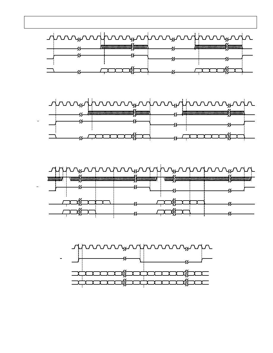
In 64-Bit Master Mode with Word Clock Output, the 16-/18-bit
words are right-justified in 32-bit fields as shown in Figures 7
and 8. The WCK output goes HI approximately with the falling
edge of the BCK output, indicating that the MSB on DATA will
be externally valid at the next BCK rising edge. The LRCK out-
put discriminates the left from the right output fields.
In 64-bit frame modes with word clock (WCK) is an input, the
16-/18-bit words can be placed in user-defined locations within
32-bit fields. This is true in both master and slave modes. The
options are illustrated in Figures 9, 10, 11, and 12. For all op-
tions, the first occurrence in a 32-bit field when the word clock
(WCK) is HI on a bit clock (BCK) falling edge will cause the
beginning of data transmission. The MSB on DATA will be
valid at the next BCK rising edge. Again, the LRCK output dis-
criminates the left from the right output fields.
Figure 9 illustrates the general case for 64-bit frame modes with
word clock input where the MSB is valid on the rising edge of
the Nth bit clock (BCK). Figures 10 and 11 illustrate the limits.
If WCK is still LO at the falling edge of the 14th bit clock (BCK)
for the AD1879 or 16th bit clock (BCK) for the AD1878, then the
MSB of the current word will be output anyway, valid at the ris-
ing edge of the 15th bit clock (BCK) in the field for the AD1879,
17th for the AD1878. This limit insures that all 16/18 bits will
be output within the current field. The effect is to right-justify
the data.
32
1
2
3
14
15
16
17
18
29
32
1
2
3
14
15
16
17
18
1
MSB
MSB≠1 MSB≠2 MSB≠3
LEFT DATA
ZEROS
LSB≠3
LSB
LSB
MSB
MSB≠1 MSB≠2 MSB≠3
RIGHT DATA
30
31
ZEROS
LSB≠2 LSB≠1
29
32
LSB≠3
LSB
30
31
LSB≠2 LSB≠1
BCK
OUTPUT
WCK
OUTPUT
LRCK
OUTPUT
PREVIOUS DATA
DATA
OUTPUT
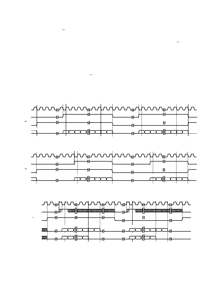
Figure 7. AD1879 64-Bit Output Timing with WCK as Output (Master Mode Only)
32
BCK
OUTPUT
1
2
3
14
15
16
17
18
29
32
1
2
3
14
15
16
17
18
1
WCK
OUTPUT
30
31
LRCK
OUTPUT
29
32
30
31
MSB MSB≠1
LEFT DATA
ZEROS
LSB≠3
LSB
PREVIOUS DATA
RIGHT DATA
ZEROS
DATA
OUTPUT
LSB
LSB≠1
LSB≠2
MSB
MSB≠1
LSB≠3
LSB
LSB≠1
LSB≠2
Figure 8. AD1878 64-Bit Frame Output Timing with WCK as Output (Master Mode Only)
LSB-2
LSB
32
BCK I/O
1
N≠1
N
N+1
31
32
WCK INPUT
AD1879
DATA OUTPUT
MSB≠1
ZEROS
LSB≠3
LRCK I/O
N+14
N+17
N+15 N+16
LSB≠1
1
N≠1
N
N+1
31
32
1
MSB
MSB≠1
ZEROS
ZEROS
LSB
LSB≠3
LSB-2
LSB≠1
AD1878
DATA OUTPUT
MSB
MSB≠1
ZEROS
LSB≠1
LSB
MSB
MSB≠1
ZEROS
ZEROS
LSB≠1
LSB
N+14
N+17
N+15 N+16
RIGHT DATA
RIGHT DATA
LEFT DATA
LEFT DATA
MSB
Figure 9. AD1878/AD1879 64-Bit Frame Output Timing with WCK as Input: WCK Transitions HI Before 16th BCK
(AD1878)/14th BCK (AD1879) (Master Mode or Slave Mode)
AD1878/AD1879
REV. 0
≠11≠
MSB
WCK INPUT
32
1
2
3
14
15
16
17
18
19
20
31
32
1
2
3
14
15
16
17
18
19
20
31
32
1
MSB≠1 MSB≠2 MSB≠3
ZEROS
LSB≠1
LSB
ZEROS
LSB
LSB
LSB≠1
BCK I/O
LRCK I/O
AD1878
DATA OUTPUT
MSB
MSB≠1 MSB≠2 MSB≠3
LEFT DATA
PREVIOUS DATA
RIGHT DATA
Figure 10. AD1878 64-Bit Frame Output Timing with WCK as Input: WCK Held LO Until 16th BCK
(Master Mode or Slave Mode)
WCK INPUT
32
1
2
3
14
15
16
17
18
19
20
31
32
1
2
3
14
15
16
17
18
19
20
31
32
1
MSB
MSB≠1 MSB≠2 MSB≠3 MSB≠4 MSB≠5
ZEROS
LSB≠1
LSB
PREVIOUS DATA
MSB
MSB≠1 MSB≠2 MSB≠3 MSB≠4 MSB≠5
ZEROS
LSB
LSB
LSB≠1
BCK I/O
LRCK I/O
AD1879
DATA OUTPUT
LEFT DATA
RIGHT DATA
Figure 11. AD1879 64-Bit Frame Output Timing with WCK as Input: WCK Held LO Until 14th BCK
(Master Mode or Slave Mode)
LSB-2
LSB-2
WCK INPUT
32
1
2
3
16
17
18
19
20
21
22
31
32
ZEROS
BCK I/O
LRCK I/O
1
2
3
31
32
RIGHT DATA
1
AD1879
DATA OUTPUT
MSB
MSB≠1
ZEROS
LSB≠3
LSB≠1
LSB
AD1878
DATA OUTPUT
MSB
MSB≠1
ZEROS
LSB≠1
LSB
ZEROS
ZEROS
MSB
MSB≠1
ZEROS
LSB≠3
LSB≠1
LSB
MSB
MSB≠1
ZEROS
LSB≠1
LSB
ZEROS
RIGHT DATA
16
17
18
19
20
21
22
LEFT DATA
LEFT DATA
Figure 12. AD1878/AD1879 64-Bit Output Frame Timing with WCK as Input: WCK Hl During 1st BCK
(Master Mode or Slave Mode)
16
1
2
3
4
5
6
15
16
LEFT DATA
MSB
MSB≠1 MSB≠2 MSB≠3 MSB≠4 MSB≠5
LSB≠3
BCK I/O
LRCK I/O
1
2
3
4
5
6
RIGHT DATA
MSB
MSB≠1 MSB≠2 MSB≠3 MSB≠4 MSB≠5
15
16
1
LSB≠2
LSB≠3 LSB≠2
AD1879
DATA OUTPUT
AD1878
DATA OUTPUT
LEFT DATA
MSB
MSB≠1 MSB≠2 MSB≠3 MSB≠4 MSB≠5
LSB-1
RIGHT DATA
MSB
MSB≠1 MSB≠2 MSB≠3 MSB≠4 MSB≠5
LSB
LSB-1
LSB
Figure 13. AD1878/AD1879 32-Bit Output Frame Timing (Master Mode or Slave Mode)
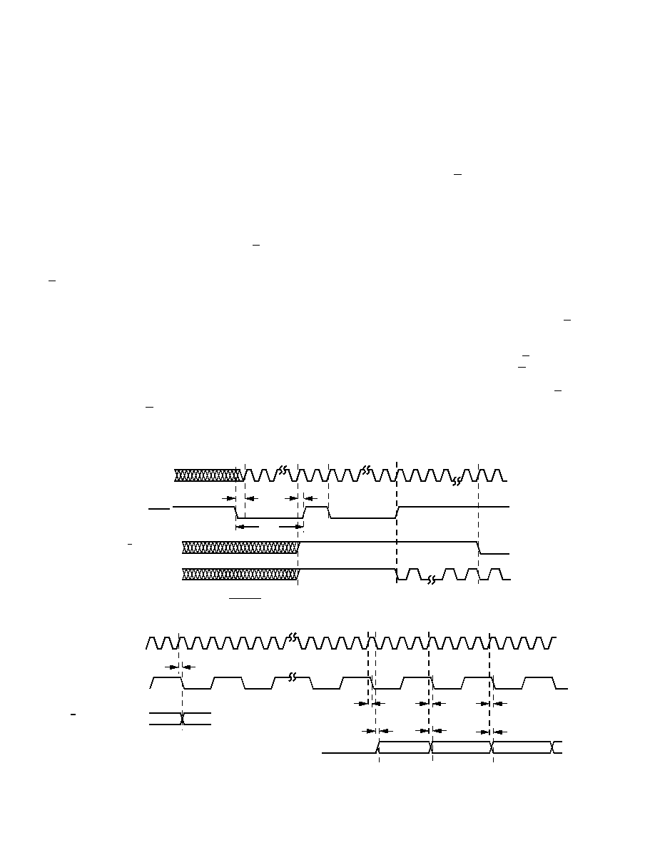
At the other limit, if the word clock (WCK) is HI during the first
bit clock (BCK) of the field, then the MSB of the output word
will be valid on the rising edge of the 2nd bit clock (BCK) as
shown in Figure 12. The effect is to delay the MSB for one bit
clock cycle into the field, making the output data compatible at
the data format level with the I
2
S data format.
In 64-bit frame modes with word clock (WCK) as an input, the
relative placement of the word clock (WCK) input can vary
from 32-bit field to 32-bit field, even within the same 64-bit
frame. For example, within a single 64-bit frame the left word
could be right-justified (by keeping WCK LO) and the right
word could be in an I
2
S-compatible data format (by having
WCK HI at the beginning of the second field).
AD1878/AD1879
REV. 0
≠12≠
delayed from a master clock input (CLOCK) rising edge by
t
DLYCK
as shown in Figure 15. The MSB of the DATA output
will be delayed from a falling edge of master clock (CLOCK) by
t
DLYD,MSB
. Subsequent bits of the DATA output in contrast will
be delayed from a rising edge of master clock (CLOCK) by
t
DLYD
. (The MSB is valid one-half CLOCK period less than the
subsequent bits.)
For master modes with word clock (WCK) inputs, bit clock
(BCK) and left/ right clock (LRCK) will be delayed from a
master clock input (CLOCK) rising edge by t
DLYCK
as shown in
Figure 16, the same delay as with word clock output modes.
The word clock (WCK) input, however, now has a setup time
requirement, t
WSET
, to the rising edge of master clock (CLOCK
at "W") and a corresponding hold time, t
WHLD
, from the rising
of the third rising edge of CLOCK (W+3) after the setup edge.
See Figure 16. As in the Master Mode--Word Clock Output
case, the MSB of the DATA output will be delayed from a fall-
ing edge of master clock (CLOCK) by t
DLYD,MSB
. Subsequent
bits of the DATA output in contrast will be delayed from a ris-
ing edge of master clock (CLOCK) by t
DLYD
.
For slave modes, bit clock (BCK) and left/right clock (LRCK)
will be inputs with setup time, t
SET
, and hold time t
HLD
,
requirements to the falling edges of CLOCK as shown in Fig-
ure 17. Note that both edges of BCK and of LRCK have setup
and hold time requirements. Note also that LRCK is setup to
the falling edge of the "L" CLOCK, coincident with the CLOCK
edge to which a falling edge of BCK is setup (B+3). LRCK's
hold time requirements are relative to the falling edge of the
"L + 31" CLOCK edge.
Also available with the AD1878/AD1879 is a 32-bit frame mode
where the 1879's 18-bit output is truncated to 16-bit words and
for both parts the output packed "tightly" into two 16-bit fields
in the 32-bit frame as shown in Figure 13. Note that the bit
clock (BCK) and data transmission (DATA) are operating at
one-half the rate as they would in the 64-bit frame modes. The
distinction between master and slave modes still holds in the
32-bit frame modes, though the word clock (WCK) becomes ir-
relevant. If "32-Bit Master Mode With Word Clock Out HI" is
selected, the word clock (WCK) will stay in a constant HI state.
If "32-Bit Master Mode With Word Clock Ignored" is selected,
the word clock pin (WCK) will be three-stated and any input to
it is ignored as meaningless. (However, such an input should be
tied off to HI or LO and not left to float.)
In both 32-bit master modes, the left/right clock (LRCK) will be
an output, indicating the difference between the left word/field
and right word/field. In 32-Bit Slave Mode, the left/right clock
(LRCK) is an input.
Timing Parameters
The AD1878/AD1879 uses its master clock, CLOCK to resyn-
chronize all inputs and outputs. The discussion above presumed
that most timing parameters are relative to the bit clock, BCK.
This is approximately true and provides an accurate model of
the sequence of timing events. However, to be more precise, we
have to specify all setup and hold times relative to CLOCK.
These are illustrated in Figures 15, 16, and 17.
For master modes with word clock (WCK) output, bit clock
(BCK), left/right clock (LRCK), and word clock (WCK) will be
t
RSET
CLOCK INPUT
RESET
t
RHLD
t
RPLS
MIN 4 CLKS
FOR SYNCH
MIN 1 CLK
MAX 2 CLKS
FOR SYNCH
MIN 4 CLKS
FOR SYNCH
1
2
3
4
126 127 128
LRCK OUTPUT
BCK OUTPUT
Figure 14. AD1878/AD1879 RESET Clock Timing for Synchronizing Master Mode WCK Output
DATA OUTPUT
BCK OUTPUT (64∑F
S
)
CLOCK INPUT
LRCK & WCK OUTPUTS
t
DLYD,MSB
PREVIOUS
NEW
MSB
MSB≠2
14
15
1
16
MSB≠1
17
t
DLYD
t
DLYD
t
DLYCK
t
DLYCK
t
DLYCK
t
DLYCK
ZEROS
Figure 15. AD1878/AD1879 Master Mode Clock Timing: WCK Output
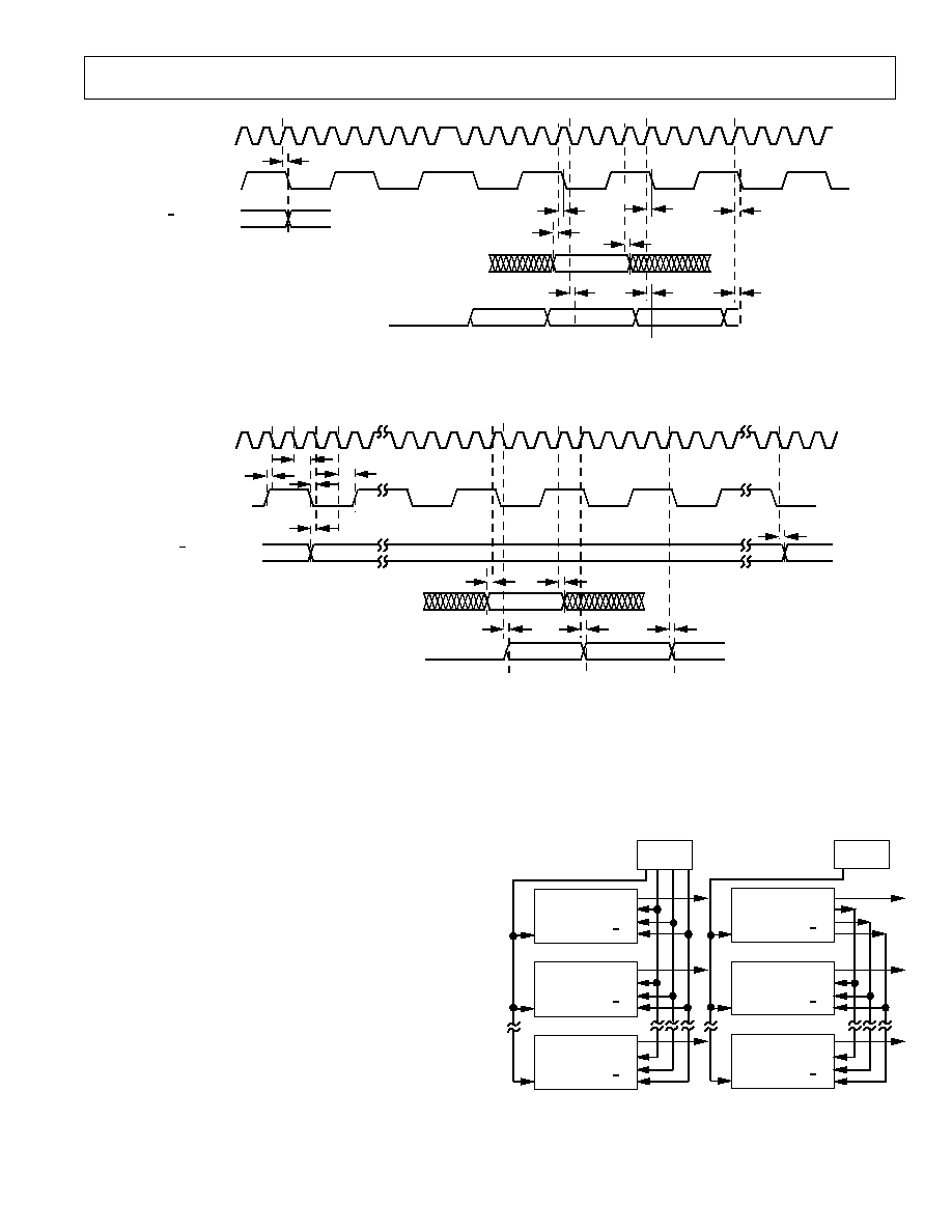
AD1878/AD1879
REV. 0
≠13≠
DATA OUTPUT
BCK OUTPUT (64∑F
S
)
CLOCK INPUT
LRCK OUTPUT
WCK INPUT
PREVIOUS
NEW
1
t
DLYCK
t
WSET
t
WHLD
t
DLYD,MSB
MSB
MSB≠2
MSB≠1
t
DLYD
t
DLYD
t
DLYCK
t
DLYCK
t
DLYCK
ZEROS
W+1 W+2 W+3
W
Figure 16. AD1878/AD1879 Master Mode Clock Timing: WCK Input
DATA OUTPUT
BCK INPUT (64∑F
S
)
CLOCK INPUT
LRCK INPUT
WCK INPUT
t
HLD
t
SET
L+1
L
W+1 W+2 W+3
W
t
WSET
t
WHLD
t
DLYD,MSB
MSB
MSB≠2
MSB≠1
t
DLYD
t
DLYD
t
SET
t
SET
t
HLD
B+1 B+2
B
B+3
L+30 L+31
t
HLD
ZEROS
Figure 17. AD1878/AD1879 Slave Mode Timing
For slave modes, the word clock (WCK) input has the same
setup time requirement, t
WSET
, to the rising edge of master
clock (CLOCK at "W" ) as in Figure 16 and a corresponding
hold time, t
WHLD
, from the rising edge of CLOCK (W+3) after
the setup edge. The MSB of the DATA output will be delayed
from a falling edge of master clock (CLOCK) by t
DLYD,MSB
.
Subsequent bits of the DATA output in contrast will be delayed
from a rising edge of master clock (CLOCK) by t
DLYD
.
Synchronizing Multiple AD1878/AD1879s
Multiple AD1878/AD1879s can be synchronized either by
making all AD1878/AD1879s serial port slaves or by making
one AD1879 the serial port master and all other AD1879s
slaves. These two options are illustrated in Figure 18.
As a third alternative, it is possible to synchronize multiple mas-
ters all in Master Mode--Word Clock Output mode. See the
"Reset" discussion above in the "Operating Features" section
for timing considerations.
AD1878/AD1879 to DSP56001 Interface
The 18-bit AD1878/AD1879 can be interfaced quite simply to
the DSP56001 Digital Signal Processor. Figure 19 illustrates
one method of connection. In this implementation, the AD1878/
AD1879 is configured to operate in 64-Bit Master Mode With
Word Clock Output. Thus, the AD1878/AD1879 is the master
of the serial interface. The AD1878/AD1879 operates indepen-
dently from the DS
µ
Ps clock. The DSP56001 serial port is
configured to operate in synchronous mode with the AD1878/
AD1879 connected to its synchronous serial interface (SSI) port.
CLOCK
SOURCE
#1
AD1879
MASTER MODE
CLK
DATA
BCK
WCK
LRCK
#2
AD1879
SLAVE MODE
CLK
DATA
BCK
WCK
LRCK
#N
AD1879
SLAVE MODE
CLK
DATA
BCK
WCK
LRCK
CLOCK
SOURCE
#1
AD1879
SLAVE MODE
CLK
DATA
BCK
WCK
LRCK
#2
AD1879
SLAVE MODE
CLK
DATA
BCK
WCK
LRCK
#N
AD1879
SLAVE MODE
CLK
DATA
BCK
WCK
LRCK
Figure 18. Synchronizing Multiple AD1878/AD1879s
AD1878/AD1879
REV. 0
≠14≠
DATA
BCK
WCK
LRCK
AD1879
SRD
SCK
SC2
SC1
DSP56001
Figure 19. AD1879 to DSP56001 Interface
To configure the DSP56001 for proper operation, the CRA
register must he programmed for a 24-bit receive data register
(RX). The CRB register must be programmed with the follow-
ing conditions: receiver enabled, normal mode, continuous
clock, word length frame synch, MSB first, SCK an input, SC1
an input and SC2 an input. The PCC register must be pro-
grammed to set the SCK, SC1, SC2, and SRD pins of Port C
to operate as a serial interface rather than in general-purpose
parallel I/O mode.
When SSI detects the rising edge of the AD1878/AD1879's
word clock (WCK), the next 24-bits on the AD1878/AD1879's
DATA pin will be clocked into the DSP56001's SSI receive
shift register on the falling edges of the inverted bit-clock
(BCK) signal. This data is then transferred to the RX register.
The 16-/18-bit word from the AD1879 will be located in Bits 8
through 23/21 of the RX register. Bits 0 through 7 will be
zero-filled. The user may poll Bit 7 (RDF) of the SSI status
register (SSISR) to detect when the data has been transferred
to RX. Alternatively, the RIE bit can be set, allowing an inter-
rupt to occur when the data has been transferred.
To differentiate left and right data, the SC1 pin of the SSI is an
input and is connected to the LRCK of the AD1878/AD1879.
After a data word is transferred to the RX register, the software
reads the IF1 bit in the SSISR, which contains the left/right in-
formation. In order to use the SC1 pin as indicated, the SSI
must operate in synchronous mode. An DSP56001 assembly
code fragment for this approach (with polling) is shown in
Table I.
Table I. DSP56001 Assembly Code for AD1878/AD1879 Data
Transfer
poll jclr
#7,X:$FFEE,poll
:loop until RX reg. has data
movep
X:$FFEF,al:
:transfer ADC to al register
jset
#I:X:$FFEE,left
:if LRCK=1, save left else
move
a1,X:$C000
:store right channel
jmp
poll
:wait for next input
left move
a1,Y:$C000
:store left channel
jump poll
If the SSI is set up for asynchronous operation, the SC0 and
SC1 pins are unavailable for left/right detection. If asynchro-
nous operation is essential, left/right information can be ob-
tained by synchronizing the AD1878/AD1879 with a software
reset. Coming out of reset, the AD1878/AD1879 will transmit
left channel data first. A flag maintained in software can main-
tain the synchronization.
AD1878/AD1879 PERFORMANCE GRAPHS
0
≠140
24k
≠80
≠120
2k
≠100
0
≠20
≠60
≠40
22k
20k
18k
16k
14k
12k
10k
8k
6k
4k
FREQUENCY ≠ Hz
dBFS
Figure 20. AD1879 S/(THD+N)--1 kHz Tone at ≠0.5 dBFS
(4k-Point FFT)
0
≠140
24k
≠80
≠120
2k
≠100
0
≠20
≠60
≠40
22k
20k
18k
16k
14k
12k
10k
8k
6k
4k
FREQUENCY ≠ Hz
dBFS
Figure 21. AD1879 S/(THD+N)--1 kHz Tone at ≠10 dBFS
(4k-Point FFT)
0
≠140
24k
≠80
≠120
2k
≠100
0
≠20
≠60
≠40
22k
20k
18k
16k
14k
12k
10k
8k
6k
4k
FREQUENCY ≠ Hz
dBFS
Figure 22. AD1879 S/(THD+N)--1 kHz Tone at ≠60 dBFS
(4k-Point FFT)
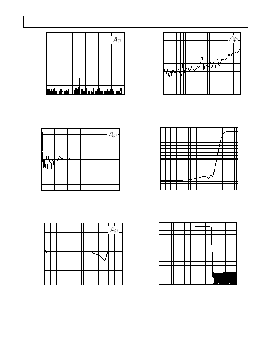
AD1878/AD1879
REV. 0
≠15≠
0
≠140
24k
≠80
≠120
2k
≠100
0
≠20
≠60
≠40
22k
20k
18k
16k
14k
12k
10k
8k
6k
4k
dBFS
FREQUENCY ≠ Hz
Figure 23. AD1879 S/(THD+N)--10 kHz Tone at ≠10 dBFS
(4k-Point FFT)
1.0
≠1.0
0
≠0.4
≠0.8
≠100
≠0.6
≠120
0.2
≠0.2
0.0
0.4
0.6
0.8
≠20
≠40
≠60
≠80
AMPLITUDE ≠ dBFS
dBFS
Figure 24. AD1879 Linearity Test--10 kHz Tone Fade to
Noise
≠64
≠68
≠90
100
100k
10k
1k
20
≠70
≠72
≠66
≠74
≠78
≠80
≠82
≠76
≠84
≠86
≠88
FREQUENCY ≠ Hz
dBFS
Figure 25. AD1878/AD1879 Common-Mode Rejection
Ratio--0 kHz to 20 kHz
≠100
≠120
≠140
100
10k
20
≠130
≠110
≠115
≠125
≠135
≠105
1k
FREQUENCY ≠ Hz
20k
dBFS
Figure 26. AD1878/AD1879 Channel Separation--0 kHz to
20 kHz
1e≠2
1e≠5
1e≠8
1e1
1e2
1M
1e5
1e4
1k
1e≠7
1u
1e≠4
1M
FREQUENCY ≠ Hz
VOLTS PER ROOT ≠ Hz
Figure 27. AD1878/AD1879 Modulator Noise Transfer
Function--0 MHz to 1 MHz
10
≠70
≠150
1e1
1e2
1M
1e5
1e4
1k
≠50
≠30
≠10
≠130
≠110
≠90
FREQUENCY ≠ Hz
dBFS
Figure 28. AD1878/AD1879 Digital Filter Signal Transfer
Function--0 MHz to 1 MHz
AD1878/AD1879
REV. 0
≠16≠
C1843≠18≠10/93
PRINTED IN U.S.A.
0
≠130
26.5
≠100
≠120
22.0
≠110
21.5
≠70
≠90
≠80
≠60
≠40
≠30
≠10
≠20
≠50
25.5
26.0
25.0
24.5
24.0
23.5
23.0
22.5
FREQUENCY ≠ kHz
DECIBELS
Figure 29. AD1878/AD1879 Digital Filter Signal Transfer
Function-- Transition Band: 21.5 kHz to 26.5 kHz
1.012
0.997
≠30
≠10
130
110
90
70
50
30
10
TEMPERATURE ≠ ∞C
GAIN
1.011
1.010
1.009
1.008
1.007
1.006
1.005
1.004
1.003
1.002
1.001
1.000
0.999
0.998
Figure 30. AD1878/AD1879 Typical Gain Over
Temperature-- ≠30
∞
C to +130
∞
C
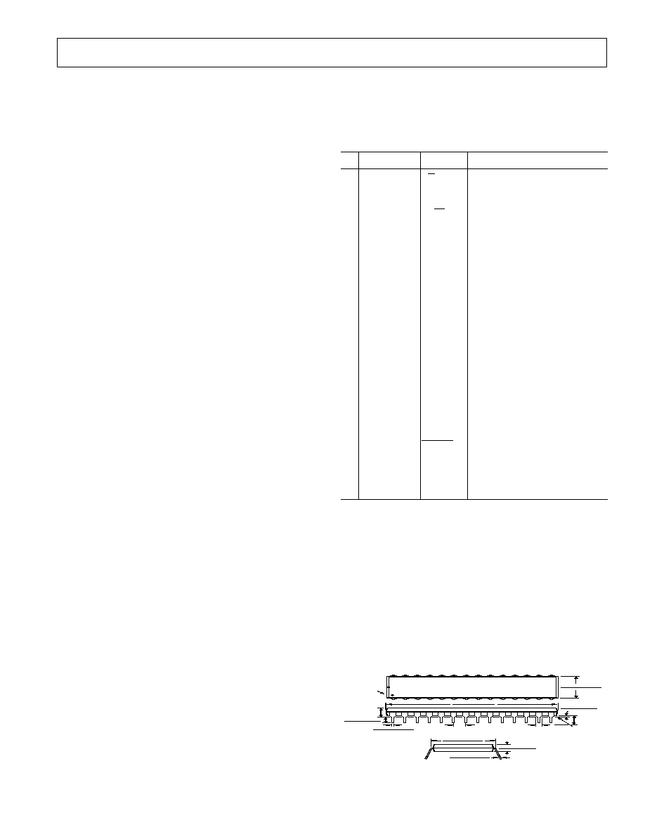
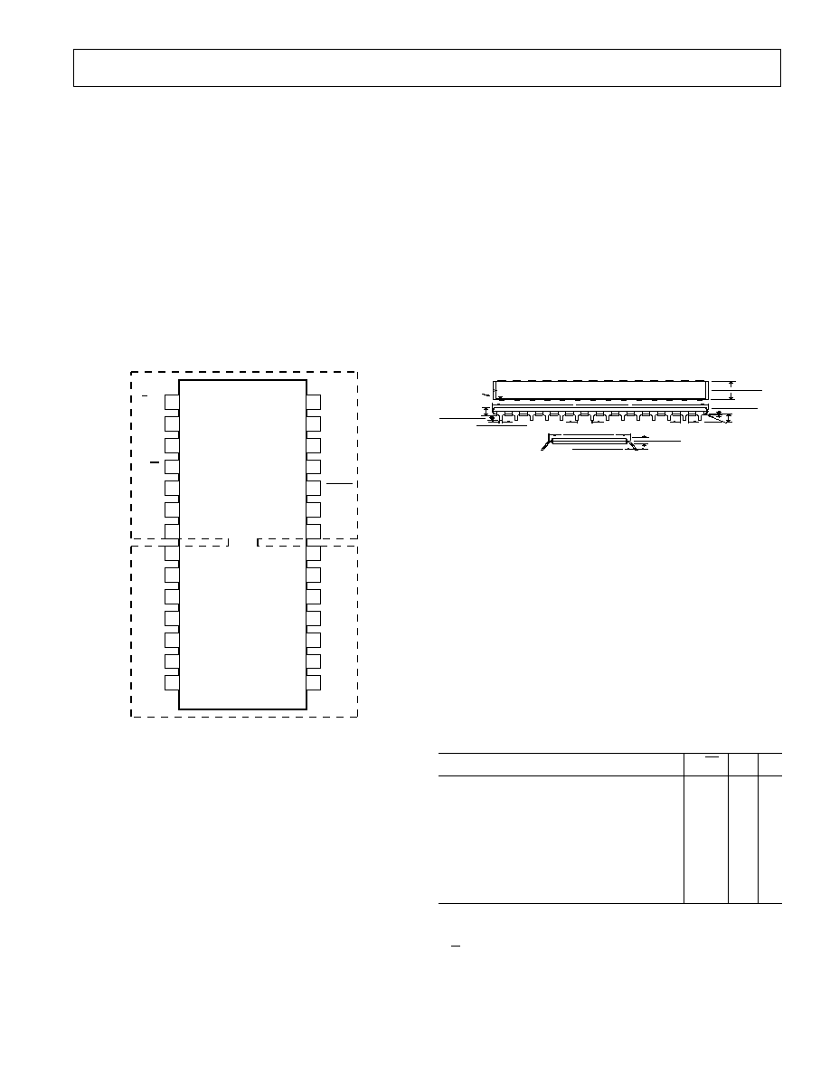
OUTLINE DIMENSIONS
Dimensions shown in inches and (mm).
D-28
28-Lead Side Brazed Ceramic DIP
0.610 (15.49)
0.500 (12.70)
14
0.100 (2.54) MAX
15
PIN 1
1
0.005 (0.13) MIN
28
0.225
(5.72)
MAX
0.200 (5.08)
0.125 (3.18)
0.026 (0.66)
0.014 (0.36)
1.490 (37.85) MAX
0.110 (2.79)
0.090 (2.29)
0.070 (1.78)
0.030 (0.76)
0.060 (1.52)
0.015 (0.38)
0.150
(3.81)
MIN
SEATING
PLANE
0.620 (15.75)
0.590 (14.99)
0.018 (0.46)
0.008 (0.20)